ANADETO Project
LLM-powered EDA
About Us
Anadeto Technology Ltd. presents ANADETO Project, an innovative EDA software that revolutionizes analog IC design with advanced large language models (LLMs) that adapt and improve over time. With ANADETO Project, users of varying experience levels can design complete integrated circuits simply by entering natural language commands, while the software leverages LLM intelligence to progressively enhance and optimize the design process. This reduces development time and costs, improves accuracy, and streamlines workflow efficiency. Experience faster, smarter, and higher-quality IC design with ANADETO Project, where intelligent automation and evolving LLM capabilities meet the power of natural language interaction, making advanced IC design accessible to all engineers.

ANADETO Project
ANADETO Project EDA revolutionizes analog IC design with breakthrough AI automation that transforms your natural language descriptions into production-ready integrated circuits.
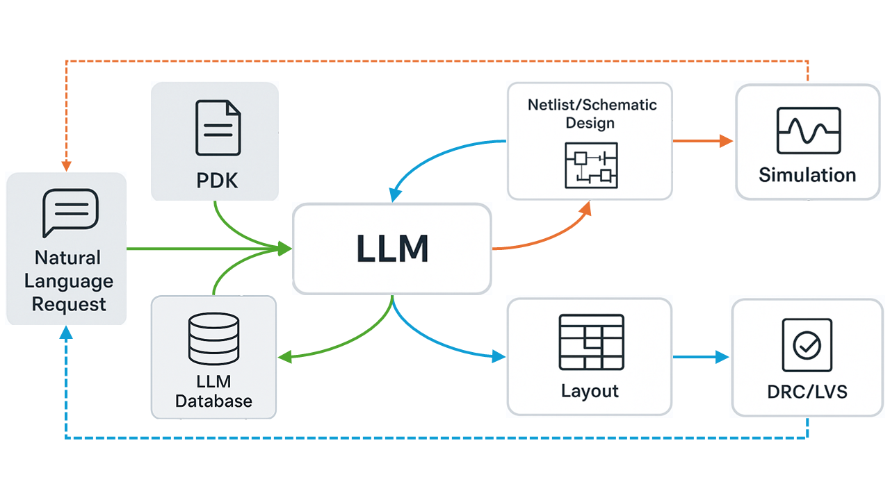
Experience an intelligent, conversational design flow where you simply describe your circuit requirements alongside your Process Design Kit (PDK), and our advanced LLM engine instantly generates hierarchical schematic/netlist and comprehensive simulation testbenches using PDK symbols and device simulation information. Watch as the system creates and automatically validates your design through circuit simulations, ensuring optimal electrical performance. Need adjustments? Simply tell ANADETO Project EDA what you'd like to improve – whether it's frequency response, power consumption, transconductance characteristics, or any other parameter. Our AI intelligently interprets your feedback and iteratively refines your design through this conversational process until you're completely satisfied. Every interaction makes our system smarter, as the LLM database continuously learns from your feedback to deliver even better results for future designs.
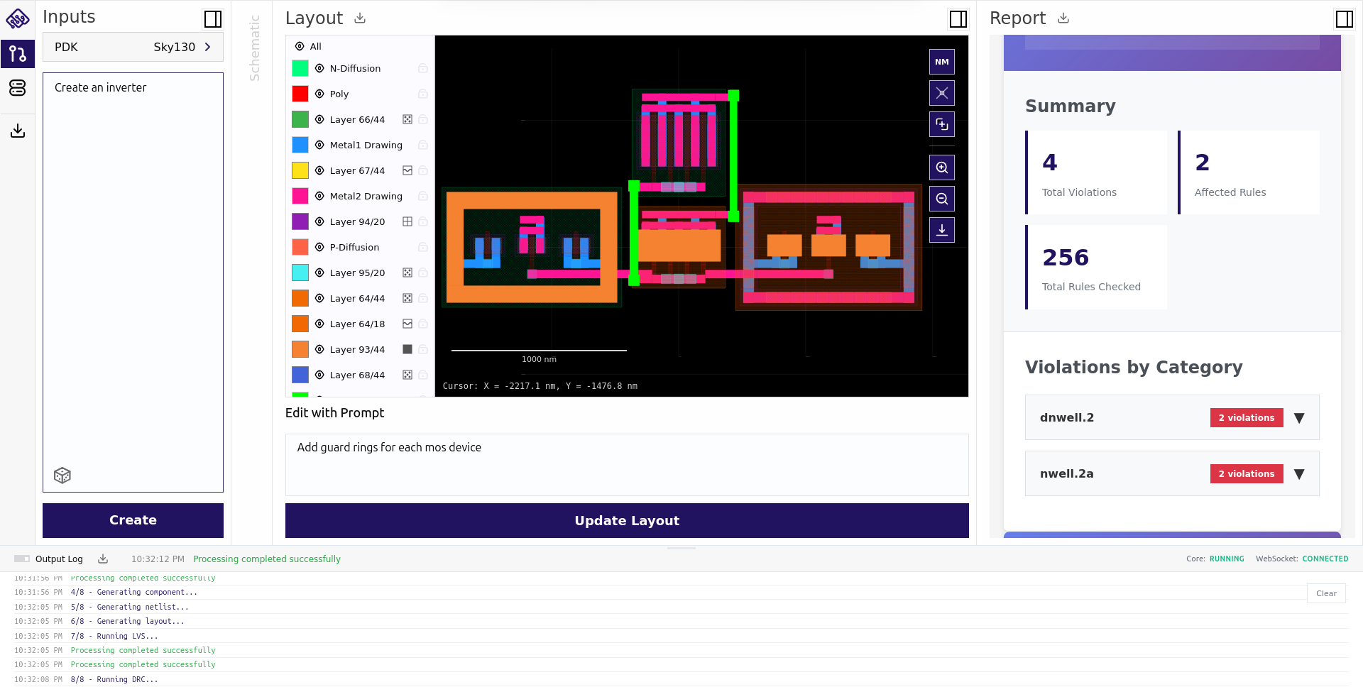
Once your circuit performs perfectly, ANADETO Project EDA seamlessly transitions to physical implementation, automatically generating hierarchical layouts with advanced placement and routing algorithms powered by PDK technology rules and layer definitions. Comprehensive Layout Versus Schematic (LVS) verification and Design Rule Check (DRC) validation ensure manufacturing-ready results. Maintain complete control over your layout with natural language feedback – optimize routing strategies, adjust device placement for matching, minimize parasitic effects, or modify metal layer utilization. This iterative optimization continues until your layout meets your exact specifications, with every refinement captured to enhance future designs.
Experience an intelligent, conversational design flow where you simply describe your circuit requirements alongside your Process Design Kit (PDK), and our advanced LLM engine instantly generates hierarchical schematic/netlist and comprehensive simulation testbenches using PDK symbols and device simulation information. Watch as the system creates and automatically validates your design through circuit simulations, ensuring optimal electrical performance. Need adjustments? Simply tell ANADETO Project EDA what you'd like to improve – whether it's frequency response, power consumption, transconductance characteristics, or any other parameter. Our AI intelligently interprets your feedback and iteratively refines your design through this conversational process until you're completely satisfied. Every interaction makes our system smarter, as the LLM database continuously learns from your feedback to deliver even better results for future designs.
Once your circuit performs perfectly, ANADETO Project EDA seamlessly transitions to physical implementation, automatically generating hierarchical layouts with advanced placement and routing algorithms powered by PDK technology rules and layer definitions. Comprehensive Layout Versus Schematic (LVS) verification and Design Rule Check (DRC) validation ensure manufacturing-ready results. Maintain complete control over your layout with natural language feedback – optimize routing strategies, adjust device placement for matching, minimize parasitic effects, or modify metal layer utilization. This iterative optimization continues until your layout meets your exact specifications, with every refinement captured to enhance future designs.
The result? Production-ready hierarchical schematic and DRC-clean, LVS-verified layout delivered in hours, not weeks. ANADETO's revolutionary automation transforms what once took experienced engineers weeks of meticulous work into an effortless, conversational experience – all while exceeding the precision and reliability standards that cutting-edge analog IC development demands.
AI That Learns
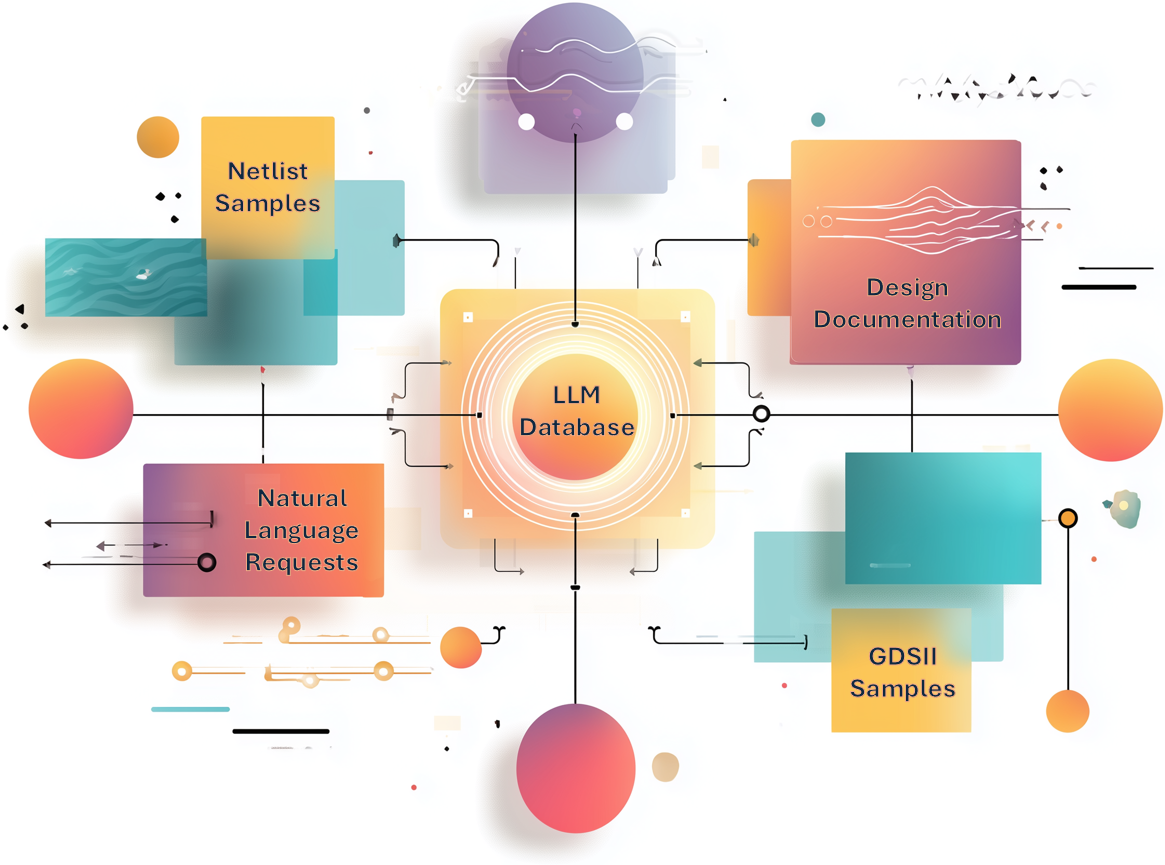
Meet the ANADETO Project's revolutionary LLM Database – your personal AI design mentor that grows smarter with every interaction. This intelligent knowledge repository captures your feedback, learns from your design decisions, and transforms your expertise into an ever-evolving foundation of analog design mastery.
Train your AI by simply using the ANADETO Project. Every optimization request, every layout refinement, every performance tweak becomes part of your personalized LLM intelligence. But why stop there? Supercharge your database by uploading proven netlists with their LVS-clean and DRC-clean GDS files, plus your design documentation and methodologies. Your years of hard-earned expertise become instant AI knowledge.
Watch the magic happen: circuits that once took multiple iterations now work perfectly on the first try. Complex design patterns that required deep experience are automatically applied. Your AI mentor evolves from assistant to master designer, embodying all your design wisdom and anticipating your needs.
This is more than automation – it's your expertise amplified. Every project makes your AI smarter, every upload expands its capabilities, every interaction builds your personalized design intelligence that works exclusively for you.
Our Roadmap
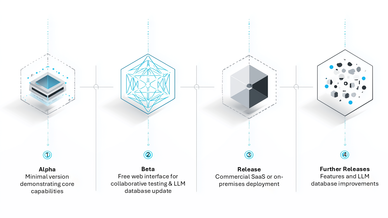
Our product will reach production through three key phases:
- Alpha Phase – A minimal but functional version showcasing the core capabilities. This stage is focused on demonstration and validation of the core technology.
- Beta Phase – Accessible via a web interface, designed to collect real-world data from institutes and organizations willing to train the software on their own IP. This phase emphasizes collaborative testing and refinement.
- Production Release – Delivered in two flexible models:
- SaaS subscription – cloud-based, easy to access and scale.
- On-premises standalone deployment – fully isolated installation at the customer’s site, with the ability for continuous retraining on customer-specific data, without internet exposure.
ANADETO Team
- Dmitri Godovsky, Dr.HabilCEOPolyn Technology Technical Founder, CTO, now Chief Scientist, Ph.D, Habil. In Physics. Author of more than 70 Scientific papers and 30 patents including IC Design, Sony, LG Electronics
- Alexey GoncharovCTOCEO at MIL team, (50 ML experts). More than 75 projects. In ML realized, PhysTech
- Max BraunEDA EngineerPrincipal EDA Engineer with more than 20 years of experience specializing in IC design automation, migration, and design enablement. An expert in developing EDA tools for semiconductor design processes across various technologies
- Kunal GhoshCBDO, Application
EngineerCadence Design Systems, Qualcomm. Now CAD tools Instructor, Professor - Howard PakoshAdviserCEO Tekstart incubator. 30+ years in Microelectronics. Founder of 5 start ups, 3 exits sold to Synopsis
- Weikai SunAdviserProfessional CAD developer, with 4 years as VP of Engineering at Synopsis
Contacts
Feel free to write and call us. We really love to communicate with our clients.
Location
📍Nikis, 26 TRANSAFRICA HOUSE, 4th Floor, 1086, Nicosia, Cyprus
📍Nikis, 26 TRANSAFRICA HOUSE, 4th Floor, 1086, Nicosia, Cyprus
By clicking the button, I acknowledge and agree that this website may store my submission in order to respond to my inquiry.

By clicking the button, I acknowledge and agree that this website may store my submission in order to respond to my inquiry.
By clicking the button, I acknowledge and agree that this website may store my submission in order to respond to my inquiry.
